- Subscribe to RSS Feed
- Mark Topic as New
- Mark Topic as Read
- Float this Topic for Current User
- Bookmark
- Subscribe
- Mute
- Printer Friendly Page
Interrupt driven high speed digital i/o with 256MB onboard memory support
01-25-2007 07:12 AM
- Mark as New
- Bookmark
- Subscribe
- Mute
- Subscribe to RSS Feed
- Permalink
- Report to a Moderator
This is in continuation of my previous post.
So over all sequence of the acquisition will be like this.
i) Application software will clear and initialize the onboard counter and enable one PFI line to activate the ADC to start the acquisition.
ii) Upon detection of signal in the detector, ADC will generate a READY signal, which is connected to one of 32 DI/O lines.
iii) On the rising edge of this signal, change detection event will be generated
iv) This will trigger two events, generation of a) ‘ DI Sample clock’ b) pulse (or change of level) on one of PFI lines
v) Due to 'DI sample clock' the one bunch of 32-bit data (out of this, only 26-bits are useful) will be transferred to system memory
vi) And due to pulse on PFI line, ADC will be reset and will become ready for the next signal
vii) Additionally when READY signal is delivered as mentioned in step (ii), the ‘cdt’ signal from ADC will be asserted to gate the 6259 onboard counter and counter starts counting.
viii) ‘cdt’ will be de-asserted after the ADC is reset as in step (vi) and counter will be stopped counting.
ix) This way acquisition will continue until it is required to stop.
x) At the end when acquisition is to be stopped, software will deactivate the PFI line (same line used in step –i) to disable the ADC and to stop the acquisition.
xi) Software will then read the content of counter to calculate total dead-time.
I hope these lines of actions are feasible in PCIe-6259. Kindly advise if some thing is wrong.
Thanks and regards
Pranav
01-25-2007 11:59 AM - edited 01-25-2007 11:59 AM
- Mark as New
- Bookmark
- Subscribe
- Mute
- Subscribe to RSS Feed
- Permalink
- Report to a Moderator
I've tested several of your questions out using an M Series DAQ device and simple DAQmx programs written in LabVIEW, and the following are my results. Some of what I've said gets into the details of programming this with the DAQmx VIs and LabVIEW, and your probably not at this point yet in your project, but I figured I would add this information for future reference and for others who read this post to get an idea of how to accomplish this.
1. Sample 26 digital lines only on every rising and/or falling edge on another digital line (your ADC's READY signal).
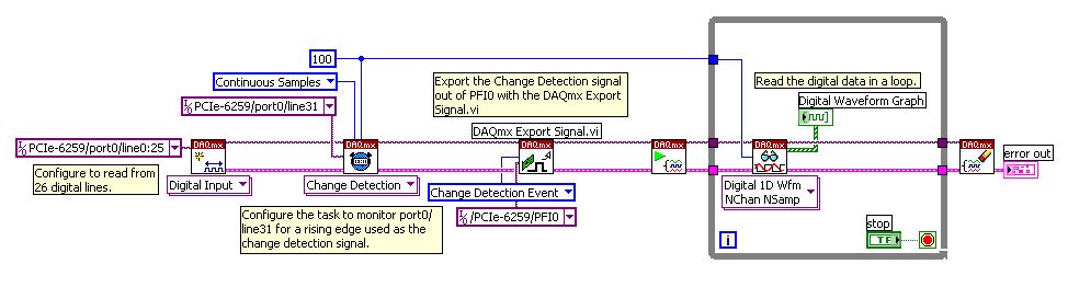
This works well with the M Series device. Sampling of the digital lines only occurs once on every active edge of the lines that are being monitored for change detection, so you are only getting one sample of the 26 digital lines for each active edge of the ADC's READY signal. The change detection events are truly used as the 'di sample clock' for the acquisition, and are not 'triggering' the acquisition of multiple samples. You can program this with the Change Detection instance of the DAQmx Timing VI, and set one or more digital lines to be monitored for rising and/or falling edges (shown below).
2. Export the Change Detection signal from the M Series device to the ADC (used as a reset signal to prepare the ADC for the next sample).
This also works well with the M Series device. I tested this by exporting the change detection event out of a PFI line on the M Series device, and monitoring that signal with a counter on another device. This change detection event is outputted as a pulse on the PFI line once for each active edge on the lines monitored for change detection. You can program this with the DAQmx Export Signal VI, and selecting the Change Detection Event and the PFI line on which to output that signal (shown below).
3. Measure the period/semi-period/pulse width of another signal (CDT signal from your ADC) with the counters on the M Series device, alongside the change detection digital input operation.
This also works well with the M Series device. There are various counter tasks you can program that compare a signal coming into a PFI line to the onboard timebase of the M Series device to make time measurements of the period or pulse width of the signal. You can program these counter operations to be buffered just like your digital task so that the measurements are stored in system memory and read into your LabVIEW program with a call to the DAQmx Read VI. I tested this out by adding a Counter Input > Period DAQmx Task to the program so that it executed alongside the digital input operation. See the shipping examples titled Meas Pulse Width-Buffered-Cont.vi for how to program this with the DAQmx VIs.
4. Turn the ADC on and off with a static digital output operation.
This also works well with the M Series device by simply adding a software-timed digital output operation to the program, and using one of the unused DIO lines. See the shipping example Write Dig Chan.vi for an example of how to do this.
So after getting more information about the details of your signaling and how you plan to interface with your ADC (the block diagram helped a lot), I am confident that the PCIe-6259 can do everything that you require. I hope this helps and let me know if you have any further questions.
Regards,
Travis G.
Applications Engineering
National Instruments
www.ni.com/support
Message Edited by Travis G. on 01-25-2007 11:59 AM
01-27-2007 06:45 AM
- Mark as New
- Bookmark
- Subscribe
- Mute
- Subscribe to RSS Feed
- Permalink
- Report to a Moderator
Dear Travis,
Many many thanks for all the important information you have passed on by actual testing of all the required functions on 6259. I am very much impressed by the support you have provided since the beginning of our discussions. I would once more say thanks to you and also to NI and Kevin as well.
Only question left is, about NI DAQmx. I hope this will be supplied with PCIe-6259 by default. OR I may need to specifically mention while ordering ? I also hope Labview's latest version(NI developer suite core edition) is enough for the development of functionality which we discussed above OR something special required ??
With warm wishes
Pranav
01-29-2007 09:57 AM
- Mark as New
- Bookmark
- Subscribe
- Mute
- Subscribe to RSS Feed
- Permalink
- Report to a Moderator
NI-DAQmx is included with any Multifunction DAQ hardware purchase. Your purchase of a PCIe-6259 will include a driver CD including DAQmx and any other drivers you may need. Additionally, the latest version of DAQmx is always available for a free download on our website. You can browse all our latest drivers by clicking Support » Drivers and Updates » Current Versions. The latest LabVIEW development suite (version 8.2) is enough for the functionality discussed above, you will need nothing else.
Good luck in your application!
Regards,
Erik J.
Applications Engineering
National Instruments
www.ni.com/support
01-29-2007 10:30 AM
- Mark as New
- Bookmark
- Subscribe
- Mute
- Subscribe to RSS Feed
- Permalink
- Report to a Moderator
Glad I could help to get you on the right path with your project. Good luck and let us know how it goes!
Travis G.
Applications Engineering
National Instruments
www.ni.com/support
03-02-2007 02:55 AM
- Mark as New
- Bookmark
- Subscribe
- Mute
- Subscribe to RSS Feed
- Permalink
- Report to a Moderator
Dear Travis,
Hello. I am little bit confused about the incoming signal rate handling capability of above mentioned strategy using e6259. In our application we decided to use ADC READY signal on one of hardware-timed i/o lines in ‘change detection’ mode for data read and one PFI line to reset the ADC. Now question is whether this type of setup will be able to handle incoming signal rate of 100k. I become little suspicious because I just read that ‘change detection’ process is an interrupt driven process and hence, may be slower. Additionally, PFI lines are not hardware-timed(?), so will it respond quick enough to reset the ADC after each data read or it will introduce 'comparatively long' delay after data is read?
Originally, this confusion started when I referred PCI-6509 for other application. 6509 has 48 static I/O, but surprisingly it also supports ‘change detection’!!! How this is possible because in static I/O mode the data read/write operation is software dependant and may not be ‘quickly’ available when ‘change detection’ is detected.
As we are in the final stage of buying both the above cards, I would like your views on these aspects .
Thanks and regards
Pranav
03-02-2007 02:59 AM
- Mark as New
- Bookmark
- Subscribe
- Mute
- Subscribe to RSS Feed
- Permalink
- Report to a Moderator
Dear Travis,
Hello. I am little bit confused about the incoming signal rate handling capability of above mentioned strategy using e6259. In our application we decided to use ADC READY signal on one of hardware-timed i/o lines in ‘change detection’ mode for data read and one PFI line to reset the ADC. Now question is whether this type of setup will be able to handle incoming signal rate of 100k. I become little suspicious because I just read that ‘change detection’ process is an interrupt driven process and hence, may be slower. Additionally, PFI lines are not hardware-timed(?), so will it respond quick enough to reset the ADC after each data read or it will introduce 'comparatively long' delay after data is read?
Originally, this confusion started when I referred PCI-6509 for other application. 6509 has 48 static I/O, but surprisingly it also supports ‘change detection’!!! How this is possible because in static I/O mode the data read/write operation is software dependant and may not be ‘quickly’ available when ‘change detection’ is detected.
As we are in the final stage of buying both the above cards, I would like your views on these aspects.
Thanks and regards
Pranav
03-04-2007 10:34 PM
- Mark as New
- Bookmark
- Subscribe
- Mute
- Subscribe to RSS Feed
- Permalink
- Report to a Moderator
Dear Travis,
Somehow my previous post has not been updated in the front page of Discussion forum/Digital I/O, so you may not have noticed. Meantime, I referred some technical notes on e6259 and found that change detection is done at quite high speed(synchronised with 80 MHz) so it may handle above incoming rate. Also I have noticed that PFI can be activated almost immidiately after DI Sample Clock. What is your comment ?
Thanks and regards
Pranav
03-05-2007
10:59 AM
- last edited on
02-16-2024
05:05 PM
by
![]() migration-bot
migration-bot
- Mark as New
- Bookmark
- Subscribe
- Mute
- Subscribe to RSS Feed
- Permalink
- Report to a Moderator
Hello Pranav,
The digital change detection event of the PCIe-6259 M Series device will transfer data to system memory using interrupts rather than DMA, and its true that this may result in a slower acquisition rate. However, I believe that with a moderatey powerful computer, you should be able to achieve change detection rates of 100kHz. The fact that the change detection is synchronized to the 80 MHz timebase basically means that that timebase is used as a sort of 'sample clock' for the change detection and this is an indication of the maximum timing resolution of the change detection event. For example, if a change on a digital line occurs between two ticks of this 80 MHz timebase, the data on the digital lines will not be latched into memory until the next tick of the 80MHz timebase. This does not directly affect how the data is transferred to system memory (whether using interrupts or DMA transfers).
Also, although PFI lines are not hardware timed, when a hardware timed signal internal to the PCIe-6259 like a change detection event is routed out of a PFI line, the consistent timing of that signal is maintained. However a small propagation delay is added to that signal due to the routing, of around 8 to 30 ns as described in the Appendix B: Timing Diagrams section of the M Series Help.
Although the interrupt driven nature of the change detection event is a concern, the PCIe-6259 is a very flexible device for routing and timing. If the change detection strategy cannot keep up with your signal rate, there is another option. The digital I/O lines on the PCIe-6259 can be clocked using correllated digital input to an internal or external timing signal, and data acquired in this fashion is transferred to system memory using DMA. What you could do is use a counter on the device to generate a single pulse, and have this counter operation be constantly retriggered by the ADC READY signal. The pulse generated by this counter can then be used as the sample clock for a correlated digital input operation, and then this correlated digital input sample clock signal can be routed out of the device through a PFI line and back to the ADC. This gets a little more complicated to program with the DAQmx VIs, but we can definitely help you out with that.
I hope this information helps,
Travis G.
03-06-2007 07:53 AM
- Mark as New
- Bookmark
- Subscribe
- Mute
- Subscribe to RSS Feed
- Permalink
- Report to a Moderator
Travis,
There was another thread I was in once regarding high-speed change detection, and I got the impression that the "Change Detection Event" signal could be used as a sampling clock just like any other hardware signal, and that transfer to system memory could still take place through DMA.
Can you double-check on the interrupts-vs.-DMA issue? Here's the thread.
-Kevin P.
