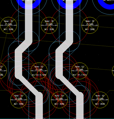
I need to route out a high density through hole connector. In order for clearance to do this I need to remove inner layer pads on pins. I can keep a 10 mil clearance from the traces to the drilled hole on the layers with p[ads removed. This should be fine and not give a clearance error, but I get massive amounts of errors when I do this. Changing all my global, trace and pad clearances to very small numbers did not help. As far as I can see there is no reason for these errors to be reported. Sample file attached. Is there any way to get these error checks to work properly? See this image of my inner layer 2 with pads removed for clearance:
