-
NI Community
- Welcome & Announcements
-
Discussion Forums
- Most Active Software Boards
- Most Active Hardware Boards
-
Additional NI Product Boards
- Academic Hardware Products (myDAQ, myRIO)
- Automotive and Embedded Networks
- DAQExpress
- DASYLab
- Digital Multimeters (DMMs) and Precision DC Sources
- Driver Development Kit (DDK)
- Dynamic Signal Acquisition
- FOUNDATION Fieldbus
- High-Speed Digitizers
- Industrial Communications
- IF-RIO
- LabVIEW Communications System Design Suite
- LabVIEW Electrical Power Toolkit
- LabVIEW Embedded
- LabVIEW for LEGO MINDSTORMS and LabVIEW for Education
- LabVIEW MathScript RT Module
- LabVIEW Web UI Builder and Data Dashboard
- MATRIXx
- Hobbyist Toolkit
- Measure
- NI Package Manager (NIPM)
- Phase Matrix Products
- RF Measurement Devices
- SignalExpress
- Signal Generators
- Switch Hardware and Software
- USRP Software Radio
- NI ELVIS
- VeriStand
- NI VideoMASTER and NI AudioMASTER
- VirtualBench
- Volume License Manager and Automated Software Installation
- VXI and VME
- Wireless Sensor Networks
- PAtools
- Special Interest Boards
- Community Documents
- Example Programs
-
User Groups
-
Local User Groups (LUGs)
- Aberdeen LabVIEW User Group (Maryland)
- Advanced LabVIEW User Group Denmark
- ASEAN LabVIEW User Group
- Automated T&M User Group Denmark
- Bangalore LUG (BlrLUG)
- Bay Area LabVIEW User Group
- British Columbia LabVIEW User Group Community
- Budapest LabVIEW User Group (BudLUG)
- Chicago LabVIEW User Group
- Chennai LUG (CHNLUG)
- CSLUG - Central South LabVIEW User Group (UK)
- Delhi NCR (NCRLUG)
- Denver - ALARM
- DutLUG - Dutch LabVIEW Usergroup
- Egypt NI Chapter
- Gainesville LabVIEW User Group
- GLA Summit - For all LabVIEW and TestStand Enthusiasts!
- GUNS
- High Desert LabVIEW User Group
- Highland Rim LabVIEW User Group
- Huntsville Alabama LabVIEW User Group
- Hyderabad LUG (HydLUG)
- Indian LabVIEW Users Group (IndLUG)
- Ireland LabVIEW User Group Community
- LabVIEW GYM
- LabVIEW LATAM
- LabVIEW Team Indonesia
- LabVIEW - University of Applied Sciences Esslingen
- LabVIEW User Group Berlin
- LabVIEW User Group Euregio
- LabVIEW User Group Munich
- LabVIEW Vietnam
- Louisville KY LabView User Group
- London LabVIEW User Group
- LUGG - LabVIEW User Group at Goddard
- LUGNuts: LabVIEW User Group for Connecticut
- LUGE - Rhône-Alpes et plus loin
- LUG of Kolkata & East India (EastLUG)
- LVUG Hamburg
- Madison LabVIEW User Group Community
- Mass Compilers
- Melbourne LabVIEW User Group
- Midlands LabVIEW User Group
- Milwaukee LabVIEW Community
- Minneapolis LabVIEW User Group
- Montreal/Quebec LabVIEW User Group Community - QLUG
- NASA LabVIEW User Group Community
- Nebraska LabVIEW User Community
- New Zealand LabVIEW Users Group
- NI UK and Ireland LabVIEW User Group
- NOBLUG - North Of Britain LabVIEW User Group
- NOCLUG
- NORDLUG Nordic LabVIEW User Group
- North Oakland County LabVIEW User Group
- Norwegian LabVIEW User Group
- NWUKLUG
- Orange County LabVIEW Community
- Orlando LabVIEW User Group
- Oregon LabVIEW User Group
- Ottawa and Montréal LabVIEW User Community
- Phoenix LabVIEW User Group (PLUG)
- Politechnika Warszawska
- PolŚl
- Rhein-Main Local User Group (RMLUG)
- Romandie LabVIEW User Group
- Rutherford Appleton Laboratory
- Sacramento Area LabVIEW User Group
- San Diego LabVIEW Users
- Sheffield LabVIEW User Group
- Silesian LabVIEW User Group (PL)
- South East Michigan LabVIEW User Group
- Southern Ontario LabVIEW User Group Community
- South Sweden LabVIEW User Group
- SoWLUG (UK)
- Space Coast Area LabVIEW User Group
- Stockholm LabVIEW User Group (STHLUG)
- Swiss LabVIEW User Group
- Swiss LabVIEW Embedded User Group
- Sydney User Group
- Top of Utah LabVIEW User Group
- UKTAG – UK Test Automation Group
- Utahns Using TestStand (UUT)
- UVLabVIEW
- VeriStand: Romania Team
- WaFL - Salt Lake City Utah USA
- Washington Community Group
- Western NY LabVIEW User Group
- Western PA LabVIEW Users
- West Sweden LabVIEW User Group
- WPAFB NI User Group
- WUELUG - Würzburg LabVIEW User Group (DE)
- Yorkshire LabVIEW User Group
- Zero Mile LUG of Nagpur (ZMLUG)
- 日本LabVIEWユーザーグループ
- [IDLE] LabVIEW User Group Stuttgart
- [IDLE] ALVIN
- [IDLE] Barcelona LabVIEW Academic User Group
- [IDLE] The Boston LabVIEW User Group Community
- [IDLE] Brazil User Group
- [IDLE] Calgary LabVIEW User Group Community
- [IDLE] CLUG : Cambridge LabVIEW User Group (UK)
- [IDLE] CLUG - Charlotte LabVIEW User Group
- [IDLE] Central Texas LabVIEW User Community
- [IDLE] Cowtown G Slingers - Fort Worth LabVIEW User Group
- [IDLE] Dallas User Group Community
- [IDLE] Grupo de Usuarios LabVIEW - Chile
- [IDLE] Indianapolis User Group
- [IDLE] Israel LabVIEW User Group
- [IDLE] LA LabVIEW User Group
- [IDLE] LabVIEW User Group Kaernten
- [IDLE] LabVIEW User Group Steiermark
- [IDLE] தமிழினி
- Academic & University Groups
-
Special Interest Groups
- Actor Framework
- Biomedical User Group
- Certified LabVIEW Architects (CLAs)
- DIY LabVIEW Crew
- LabVIEW APIs
- LabVIEW Champions
- LabVIEW Development Best Practices
- LabVIEW Web Development
- NI Labs
- NI Linux Real-Time
- NI Tools Network Developer Center
- UI Interest Group
- VI Analyzer Enthusiasts
- [Archive] Multisim Custom Simulation Analyses and Instruments
- [Archive] NI Circuit Design Community
- [Archive] NI VeriStand Add-Ons
- [Archive] Reference Design Portal
- [Archive] Volume License Agreement Community
- 3D Vision
- Continuous Integration
- G#
- GDS(Goop Development Suite)
- GPU Computing
- Hardware Developers Community - NI sbRIO & SOM
- JKI State Machine Objects
- LabVIEW Architects Forum
- LabVIEW Channel Wires
- LabVIEW Cloud Toolkits
- Linux Users
- Unit Testing Group
- Distributed Control & Automation Framework (DCAF)
- User Group Resource Center
- User Group Advisory Council
- LabVIEW FPGA Developer Center
- AR Drone Toolkit for LabVIEW - LVH
- Driver Development Kit (DDK) Programmers
- Hidden Gems in vi.lib
- myRIO Balancing Robot
- ROS for LabVIEW(TM) Software
- LabVIEW Project Providers
- Power Electronics Development Center
- LabVIEW Digest Programming Challenges
- Python and NI
- LabVIEW Automotive Ethernet
- NI Web Technology Lead User Group
- QControl Enthusiasts
- Lab Software
- User Group Leaders Network
- CMC Driver Framework
- JDP Science Tools
- LabVIEW in Finance
- Nonlinear Fitting
- Git User Group
- Test System Security
- Developers Using TestStand
- Product Groups
- Partner Groups
-
Local User Groups (LUGs)
-
Idea Exchange
- Data Acquisition Idea Exchange
- DIAdem Idea Exchange
- LabVIEW Idea Exchange
- LabVIEW FPGA Idea Exchange
- LabVIEW Real-Time Idea Exchange
- LabWindows/CVI Idea Exchange
- Multisim and Ultiboard Idea Exchange
- NI Measurement Studio Idea Exchange
- NI Package Management Idea Exchange
- NI TestStand Idea Exchange
- PXI and Instrumentation Idea Exchange
- Vision Idea Exchange
- Additional NI Software Idea Exchange
- Blogs
- Events & Competitions
- Optimal+
- Regional Communities
- NI Partner Hub
-
 bikeron
on:
New International Rectifier Components in Multisim 14.0
bikeron
on:
New International Rectifier Components in Multisim 14.0
-
 giondoo77
on:
Creating Custom Arduino Shields With NI Multisim
giondoo77
on:
Creating Custom Arduino Shields With NI Multisim
- robo_Jeff on: Multisim Touch for iPad Now Available
-
doa4378
on:
New Models for Photovoltaic Cells in Multisim
- Mahmoud_W on: Connectors for NI 78xxR Multifunction RIO series in Multisim
- Mahmoud_W on: Search for Components in Digi-Key's Database While Building Your Circuit in Multisim
- BMac on: Ultiboard Mating PCB Design of the new NI GPIC Platform for Energy Applications
-
Henry_Lavery
on:
Automotive Application: Hall Effect Sensor in Multisim
- GarretF on: LabVIEW-Multisim Co-Simulation with Variants and Hierarchical Blocks (Part 2)
-
Control_Dir
on:
Adding 3D Information in Ultiboard
Integrating AWR Microwave Office Designs into NI Multisim
- Subscribe to RSS Feed
- Mark as New
- Mark as Read
- Bookmark
- Subscribe
- Printer Friendly Page
- Report to a Moderator
Hello Circuit Designers,
I would like to share with you a new proof of concept design that takes advantage of multiple NI tools. The design is a Low Noise Amplifier (LNA) operating at 10 GHz fully analyzed in AWR's Microwave Office. Along with the LNA, a peripheral low-frequency circuit providing the needed bias levels for the FET is simulated in NI Multisim. Finally, the LNA is imported into Multisim as a footprint only component to be combined with the bias circuit. A final PCB prototype of the complete system is created using NI Ultiboard.
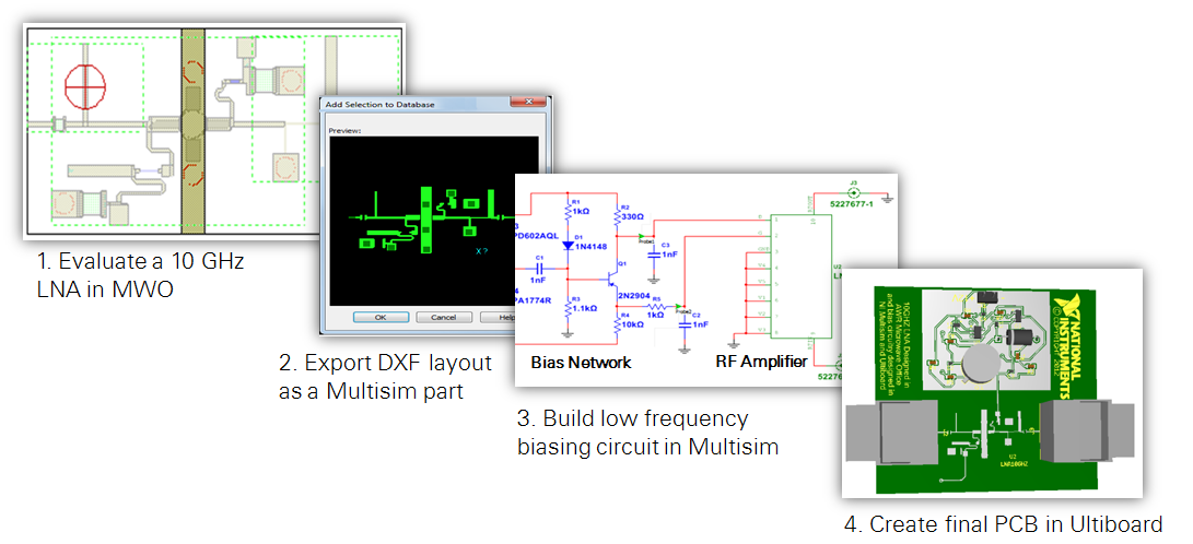
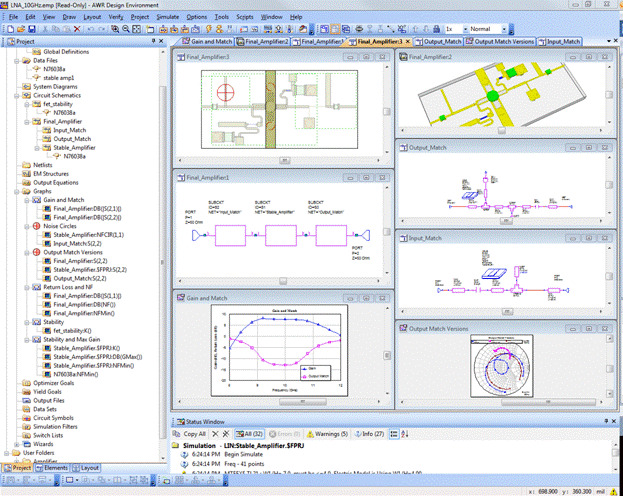
1. Evaluation of the 10 GHz LNA performance in MWO
This design of a 10 GHz LNA built on 10 mil alumina is using a NEC 76038 GaAs MESFET. Running the analysis of the circuit, you learn that the LNA has 7.7dB gain and 2.15dB NF at 10 GHz.
Designing this amplifier in MWO you can take advantages of the real-time tuning, frequency subset Smith Chart plots of noise and matching circles, and the X-Models for discontinuities accuracy to validate the performance of the amplifier.
2. Creation of a LNA footprint component to use in Multisim
This step means to export the layout of this LNA in a DXF format and integrate it into Multisim as a new component.
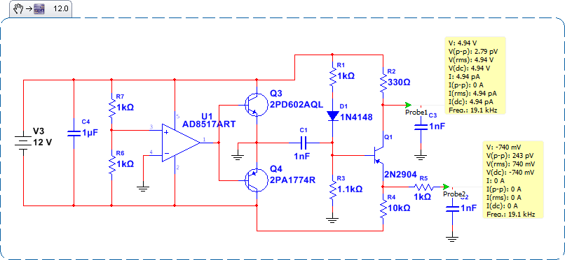
3. Design of low frequency bias network in Multisim
The next step in this example is to accurately validate the circuit performance of a biasing circuit that takes a 12VDC input and outputs 2 arbitrary voltage levels for Gate and Drain biasing of the MESFET at -0.7V and 5V respectively. Eventually this bias circuit will be integrated with the LNA on a single PCB.
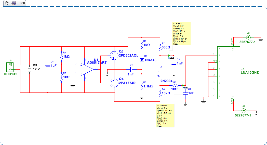
4. Prototyping the complete system in Ultiboard
Finally, the LNA component is added to the Multisim design and a final PCB layout is created using Ultiboard.


Let me know if you have ideas for similar use-cases.
Mahmoud W
National Instruments
You must be a registered user to add a comment. If you've already registered, sign in. Otherwise, register and sign in.
