NI Circuit Design Community Blog

Community Browser
Labels
cancel
Showing results for 
Search instead for 
Did you mean: 
MahtabZ
13652 Views
0 Comments

When designing a PCB, it can be difficult to picture what a board will look like once it has been manufactured, simply by seeing a 2-dimensional representation of it.


Engineers can use the 3D view in Ultiboard to gain intuition with respect to the dimension of height. One can see how a board will look when manufactured, and understand the height of components.


Most of the components in Ultiboard have a 3D model defined that can be viewed in this intuitive way to provide further analysis into the design of a PCB.


Let’s open a sample design in Ultiboard. Go to File>>Open Samples… and navigate to the Getting Started folder. Open the Getting Started file and click the GS4 tab. This is what you should see:

figure1.PNG

Figure 1: Getting Started sample design

Now from the toolbar go to Tools>>View 3D, and a new tab will open with a 3D view of the design.

figure2.PNG

Figure 2: 3D view of the design

Navigating the 3-dimensional circuit board is easy! Just left-click and hold down the mouse anywhere in the 3D view, and move the mouse. The board will rotate and move according to the mouse movements.  You can also zoom in or out of the 3D view using the scroll button on your mouse.

If you want to see the height of your components, go to Tools>>Show/Hide Height. Click on any component and a yellow arrow and a number will appear over it. This data represents the height of that component from the top board layer.

MahtabZ
12877 Views
0 Comments

This week, I present to you another trivia question.  Name the function of this circuit (for example, Output = A + B + CD):

cmos mystery.PNG

Once again, feel free to use Multisim to help you out.  I look forward to hearing your responses in the comments!

Until next week,

Mahtab

MahtabZ
12697 Views
0 Comments

National Instruments is hosting NIWeek, the industry's premier event on graphical system design that attracts more than 3,000 of the world's brightest engineers, educators, students, and scientists.


NIWeek 2011 opens August 1 at the Austin Convention Center in Austin, Texas, for four days of interactive technical sessions, targeted summits, hands-on workshops, and exhibitions on the latest developments for design, control, automation, manufacturing, and test. 


A few weeks ago I promised you an inside look at NIWeek, so I have compiled some of the Academic Technical Sessions that you may find particularly interesting:


Using NI ELVIS, Multisim, LabVIEW, and NI myDAQ in Electronics and Electrical Engineering

Learn how the University of Manchester incorporates hands-on learning throughout the curriculum. Using the National Instruments Educational Laboratory Virtual Instrumentation Suite (NI ELVIS), NI myDAQ, Multisim, and LabVIEW, Dr. Danielle George discusses how students implemented a dynamic learning environment for students in the lecture course, in the laboratory, and off campus.


Waterloo Labs Showcase

Four NI summer interns have been building low-cost projects and sharing them with the world over YouTube to the delight of the student, hobbyist, and tinkerer communities. Meet the team and see what they have been up to, what challenges they faced, and how they pulled off these projects.


You may recognize Waterloo Labs as the Engineers who brought us cool projects like “Play NES with your eyes”:


Biomedical Engineering: Measurements to Design

The University of Michigan biomedical engineering program has created a measurements-to-design sequence of courses to train students on LabVIEW in the measurements course and help them create solutions for the medical school in their senior design and masters design courses.


Using CompactRIO to Teach Renewable Energy Concepts

Learn how United Arab Emirates (UAE) University is incorporating graphical system design to teach and reinforce key green engineering concepts such as building integrated photovoltaic systems. Explore how students build a real-world replica of a house and use technologies such as CompactRIO with LabVIEW to monitor photovoltaic arrays for performance and fault detection.


LabVIEW Robotics Starter Kit (DaNI) Lab Exercises

DaNI is a preassembled robot that uses LabVIEW and existing libraries to quickly create a moving, sensing robotic vehicle. Students can focus more on learning various robotics concepts such as obstacle avoidance, localization, and path planning. Learn about the development of these lab exercises and the results of the first class that used them, and view a demo of the exercises.

MahtabZ
19170 Views
0 Comments

NI Multisim offers many simulation-driven instruments that are fully interactive. They allow you to change settings while running a simulation, and see the new results instantly.

Let’s take a look at the simulated vendor instruments from Agilent and Tektronix. Place the components from the Instruments toolbar (Simulate>>Instruments), wire it into your circuit, and double-click the instrument to see the front panel. In figures 1 and 2, you can see the front panel of the Agilent and Tektronix oscilloscopes, respectively.

figure1.PNG

Figure 1: Agilent Oscilloscope

figure2.PNG

Figure 2: Tektronix Oscilloscope

These instruments work just like the ones on your lab bench, including the need to turn them on using the POWER button! You can click the buttons and turn the dials, just as you would on a real oscilloscope. In figure 3, I have changed the SEC/DIV dial on the far right side of the instrument, and you can see the new results on the screen.

figure3.PNG

Figure 3: Tektronix Oscilloscope with new SEC/DIV value

Test it out for yourself! I have made an RLC circuit, shown in figure 4, and hooked up the Tektronix Oscilloscope – the input to channel 1, and the output to channel 2.

figure4.PNG

Figure 4: RLC Circuit

Next I double-click the Tektronix Oscilloscope, click the POWER button, and run the simulation. At first you may not see anything, so click the CH 1 MENU and CH 2 MENU.  After playing around with each VOLTS/DIV and the SEC/DIV, you should see something similar to figure 5.

figure5.PNG

Figure 5: Simulation results shown on the Tektronix Oscilloscope

MahtabZ
12877 Views
0 Comments

Congratulations to normandinf for solving last week’s trivia question!  There were quite a few responses on our Facebook page as well, and everyone knew that the circuit was a High-pass filter.  Good job everyone!

For those of you who were stumped, here is the solution.  With the circuit open in Multisim, go to the toolbar and click Simulate>>Analyses>>AC Analysis. I have my analysis configured as shown in Figure 1.

Figure1.PNG

Figure 1: AC Analysis Frequency parameters

In the Output tab, add V(output) into the selected variables for analysis, as in figure 2.

Figure2.PNG

Figure 2: AC Analysis Output

Click Simulate and you’ll see something similar to figure 3.

Figure3.PNG

Figure 3: AC Analysis simulation

So, we can clearly see that it is a high-pass filter. To find the cut-off frequency, we can use the cursors to find that the -3 dB frequency is about 1.59 kHz. But what is that little dip on the end, after the 10MHz range?  Let’s take a closer look, by increasing our frequency range in our analysis. Figure 4 shows the new frequency range.

Figure4.PNG

Figure 4: AC Analysis, new frequency range

When we simulate, now we see something a little more confusing, shown in figure 5.

Figure5.PNG

Figure 5: AC Analysis simulation with larger frequency range

When I first saw this, I was a bit confused. I had specifically looked up the configuration of a high-pass filter and built one,and yet – here was what seemed to be a band-pass filter staring me in the face.So which is it? A high-pass filter, or a band-pass filter?

The answer lies in the fact that the circuit is an active high-pass filter, and the maximum pass band frequency is determined by the characteristics of the op-amp I used. So normandinf was absolutely right when he said there was a gain of -2 at high frequencies.

I hope you enjoyed trying to solve last week’s trivia question, and I hope this post was educational! I know I learned a lot.

Mahtab

MahtabZ
12870 Views
1 Comment

Hello everyone,

Today I’ve got a bit of a mystery circuit for you to solve!  The first person to get the right answer gets bragging rights, plus a special mention in my blog post next week .

So here it is: What type of filter is this?  And for bonus marks, what is/are the cutoff frequency/frequencies? mystery filter.PNG

Oh, and feel free to use Multisim to help you out! I’ll post the answer next week.

For my next blog post, I am planning on giving you all some insider information into NI Week this year (more info here). So stay tuned!

Mahtab

MahtabZ
13593 Views
0 Comments

Hello again!

This week I’m going to share a tip for making your circuit files look a little more professional.  Use Title Blocks on each of your designs, and you can have a fully customizable and standardized label for all of the circuits you design. You can see an example of a Title Block in Figure 1.

Figure1.PNG
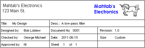
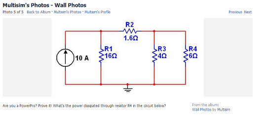
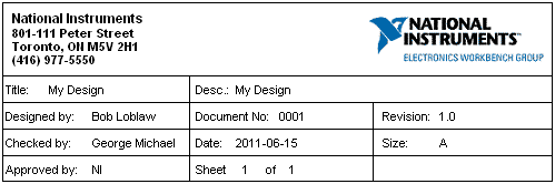
Figure 1: Sample Title Block
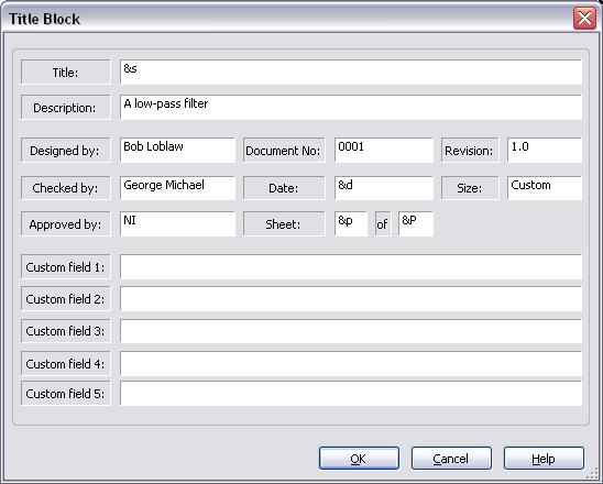
Title Blocks are easy to customize.  From the toolbar, go to Place>>Title Block. You will be directed to the titleblocks folder, where several template designs are provided. For my design, I chose default.tb7. The Title Block is ghosted to your mouse, so click anywhere on the screen to place it.

Now you can fill in the various fields to describe your design. Some of these fields, like “Title”, will be filled in automatically based on the file name. Double-click the Title Block to open the Title Block window as shown in Figure 2.

Figure2.PNG

Figure 2: Title Block window

Once you have filled in the fields, click OK and you are taken back to the circuit.  Right-click the Title Block and click Move to>>Bottom Left to align it to the bottom left side of the screen.  My completed design is shown in Figure 3.

Figure3.PNG

Figure 3: Complete design with Title Block

You may not work at National Instruments, so it makes sense that you would change the graphic shown in the top right hand corner of the Title Block. Right-click the Title Block and select Edit Symbol/Title Block. This will open up the Title Block Editor. You can delete the National Instruments logo and place your own. In the toolbar of the Title Block Editor, go to Graphics>>Bitmap… and navigate to a saved image that you want to use. Make any changes, and save the title block file in a folder (you will remember!) so you can use it again for other circuit files.

As an example, my finished Title Block is shown in Figure 4.

Figure4.PNG

Figure 4: Modified Title Block

Now that you have your customized Title Block file, you can use this for every circuit file you make.

What methods have you used in Multisim to make your files look more professional? Leave a comment!

Thanks for reading,

Mahtab

MahtabZ
21188 Views
0 Comments

Hello all,

As an Engineering student, I have a pretty heavy workload.  As such, I’m always looking for tools to help me recall details about my courses or labs. That’s why I was delighted when I found out about the Circuit Wizard in Multisim.

Let me paint a picture for you. You have an electronics lab session in a few hours, and you’re feverishly trying to complete the preparation work. The first part of the lab asks you to design a non-inverting amplifier, and the whole lab is dependent on this step. Panicking, you realize you’ve completely forgotten what the configuration of a non-inverting amplifier is.

Lucky for you, Multisim comes with a tool called the “Circuit Wizard”. I have found that this feature is especially helpful when I can't remember small details about common circuits. Here’s a demonstration of how it works:

From the toolbar in Multisim, go to Tools>>Circuit Wizards>>Opamp Wizard. The Opamp Wizard window, shown in Figure 1, will open. You can now choose the Type of Opamp (in our case, Non-inverting amplifier) and details about the circuit, such as the Input Voltage (Pk), Input Frequency, and Voltage Gain (Av). Click Verify, and then Build circuit.

Figure1.PNG

Figure 1: Opamp Wizard window

The circuit is ghosted to your mouse. Click anywhere on the page to place your design, and voilà! You have a non-inverting amplifier with a gain of 5, as shown in Figure 2. You can test it out for yourself - Garret already taught us the fastest way to calculate the gain­ in a previous blog post.

Figure2.PNG

Figure 2: Non-inverting amplifier circuit

The Circuit Wizard can also build other types of circuits – there is a 555 Timer Wizard, a Filter Wizard, and a CE BJT Amplifier Wizard. Experiment with these, and in no time you’ll become a circuit wizard yourself!

See you next week,

Mahtab

MahtabZ
15973 Views
0 Comments

Hello again!

In keeping with my goal of offering helpful advice to Multisim and Ultiboard users, this week’s blog post will be on a handy tool that Multisim offers – generating reports; specifically, a Bill of Materials report. This useful tool is an aid in the manufacturing process.  It lists the components used in your design, and provides a summary of the components needed to manufacture the circuit board.

To generate a Bill of Materials report for your circuit file, select Reports>>Bill of Materials.  The Bill of Materials window will open, as shown in Figure 1.

figure1.PNG

Figure 1: Bill of Materials window

As you can see, this report lists each component’s Quantity, Description (including the type of component and its value), RefDes, Package (footprint), and Type.

A useful feature of the Bill of Materials report is “Export to Microsoft Excel” (4th button along the top of the window). This gives you an Excel file that you can print, save, or send to colleagues.

You can even add your own User Fields, which will show up as extra columns in the Bill of Materials report. To do this, go  to Tools>>Database>>Database Manager. Click the User field titles tab. From here, you can add or delete user fields. I am going to add a new field called “Max Temp”, as in Figure 2.

figure2.PNG

Figure 2: Adding new user fields

If we click Close and return to the Bill of Materials report (Reports>>Bill of Materials), we can see that the new user field “Max Temp” is a column, shown in Figure 3.

figure3.PNG

Figure 3: Bill of Materials report withour new user field

Now “Max Temp” is an attribute of every component in our design, and I can change the Max Temp attribute of any component in my database. Once again, go to Tools>>Database>>Database Manager and click the Components tab. Choose the desired partfrom the database and scroll to the right until you can see the “Max Temp” column. As you can see in Figure 4, I can change the value of this attribute formy chosen component.  This value is saved with the component in the database for use in other files, as well.

figure4.PNG

Figure 4: Changing the Max Tempattribute of a component

Alternatively, you can just right-click any component already placed in your design and choose Properties. Go to the User fields tab and change the value of Max Temp there.

I hope this mini-tutorial on the Bill of Materials report in Multisim has been helpful.  Thanks for reading!

Mahtab

MahtabZ
25895 Views
5 Comments

Hi everyone!  My name is Mahtab, and I am the newest addition to the NI Team.  I am studying Engineering at the University of Toronto, and have some great experience using Multisim and Ultiboard. Throughout this summer I will be contributing to this blog on a weekly basis.  My goal is to use my experience with simulation, circuit design and Multisim, coupled with my unique perspective as a student at the University of Toronto, to write helpful posts on how to be more productive when using our NI tools. I look forward to your feedback and thoughts!


A few weeks ago, Fernando made a post that dealt with how to create a component based upon a SPICE model downloaded from the manufacturer’s website.  But what do you do in the instances when a manufacturer has not (or cannot) provided a SPICE model for their product?  Is it still possible to create a custom component?


Fortunately, this is possible in Multisim, and there are a few ways of doing it.  One way is to create a SPICE macro model for an IC (a very good tutorial can be found here). Another way, which I will explain today, is to use the Multisim Model Maker, a seldom used tool in the product. Because the SPICE model created by this tool is basic, accuracy cannot be guaranteed. Nevertheless, it is a fast and easy way to create a simple SPICE model.


For this tutorial, I am going to create the TZX2V4A Zener Diode from Vishay (available at http://www.vishay.com/diodes/list/product-85614/).  As you can see from the website, the simulation model is not available, but a datasheet is.  With the values given on the datasheet, and only these values, we will be able to create our component. In just 8 simple steps (and about 5 minutes of work) we will create a custom diode!


Step 1:

From the toolbar, go to Tools>>Component Wizard.  The Multisim Component Wizard will walk you through the steps of creating a component. Fill out Step 1 so it looks similar to Figure 1:

Figure1.PNG

Figure 1 - Component Wizard Step 1


Click Next to go to Step 2, which asks for a footprint.


Step 2:

Click the Select a footprint button and then the Filter button and fill out the fields as shown in Figure 2. Note that you will need to click the Add row button to create each filter.

Figure2.PNG

Figure 2 – Component Wizard Footprint Filter


Click Ok to go back to the footprint selection step. It should look similar to Figure 3.

Figure3.PNG

Figure 3 – Select a Footprint


Click Select to confirm the footprint, and you will be brought back to Step 2 of the Component Wizard. In our case, we are working with a Single Section Component, and the Number of pins is 2.  Click Next.


Step 3:

Here, we specify a symbol.  The default is the rectangle shown, but we are going to change the symbol so it actually looks like a Zener Diode. Click Copy from DB and select any Zener Diode from the Master Database (under the Diode group, Zener family), then click OK (as in Figure 4 below).

Figure4.PNG

Figure 4 – Symbol Information


Click Next.


Step 4:

Accept the defaults and click Next.


Step 5:

Change the Footprint pins so that the symbol and footprint pins have the same mapping as in Figure 5.

Figure5.PNG

Figure 5 - Mapping information


Click Next.


Step 6:

In this step of the Component Wizard, we are asked for Model Data. If we had a SPICE model we could copy it here; since one is unavailable, however, we can simply use the Model Maker. Click the Model Maker button, and select Zener from the list. Click Accept.


Now, we can use the values from our datasheet to fill in the Electrical Characteristics and the Temperature Coefficient, Capacitance if that data is available. Fill in the appropriate values. In our case, it should look similar to the following image (based upon our datasheet):

Figure6.PNG

Figure 6 - Zener Model


Click Ok when you have filled in all the data. The values you enter may be different from the above image depending on which component you are creating.


Now we are back to Step 6 of the Component Wizard, and you can see that the Model data has been (magically) filled in. Change the Model name to TZX2V4A and click Next.


Step 7:

Accept the defaults and click Next.


Step 8:

Now we choose a location in the database for our new component.  I am going to place it in the User Database, under Diodes.  Click the Add Family button and call the family name Zener. Click Ok, select the Zener family you just created, and click Finish.

Figure7.PNG

Figure 7 - Component Wizard Step 8

And there you have it – you have created a component using the Multisim Model Maker.  You can now test your component by building a test circuit.

Thanks for tuning in!

Mahtab

Bhavesh
13009 Views
0 Comments

Hello All,

It is always exciting for me to get news about NI products winning awards - howevr since my career has been closely tied to NI Multisim - it is always particularly exciting when I see NI Multisim win a kudo from the EDA community. I was happy to once more make my way to the APEX conference (again held in Las Vegas) to witness Multisim receiving recognition at the New Product Innovation Awards Ceremony (held by UP Media). We here at National Instruments continue to focus on our strategy to have tools, resources and employees to make engineers throughout the world successful; Having an award winning product helps to communicate that very strategy!

Although I was unlucky at my 5 minutes at the Blackjack tables, I did come away from APEX with not one, but TWO awards for NI Multisim. Multisim won awards for:

  1. 2011 "Best System Modelling & Simulation Tools": NI Multisim 11.0.1 (released October 2011) [ This makes it 2 years in a row! ]
  2. 2011 Best "Design Verification Tool": NI Multisim Component Evaluator - Analog Devices Edition (released December 2011)

As you can imagine our R&D, Marketing and Sales teams are ecstatic at this news! . You can check out my previous blog on the Design Verification Tools win in 2010 here.

NI Multisim Component Evaluator - Analog Devices Edition is a brand new version of Multisim that is available for free use by Analog Devices customer. This version is different from our standard tool, which is a design tool, and instead focusses on allowing engineers to take common ADI components and evaluate their performance. NI Multisim Component Evaluator is one part of Analog Devices holistic approach to choosing semiconductor products. Whether you are using web tools to understand design needs at analog.com, or using Multisim to develop small evaluation circuits, ADI are able to provide engineers with tools that effetively transition a customer through the device decision process.Ultimately this can ensure that engineers are making the decisions to make better decisions, be more productive, and ultimately be more successful!

Mike Beutow, editor-in-chief of PCD&F commented that “We saw some true innovation this year. The judges were truly impressed with the quality of the entries.” As we here at NI have been discussing for many years - simulation is a powerful tool, empowering engineers to make better design decision. Whether at the component evaluation stage, or for actual design work with NI Multisim - we feel we can help to reduce errors or improve performance.

For the sake of slight self promotion (I promise this will be the only time ) - you can see a picture of me accepting one of the two awards from Mike in Vegas. However I must be truly honest that the real kudos should go to our incredible R&D team that continue to develop the tools that make engineers successful throughout the design flow.

Thanks for reading!

Bhavesh Mistry

General Manager - National Instruments Toronto

P.S. I hope that you all take the opportunity to read our blog throughout the summer. We will have brand new content from Fernando Dominguez and Mahtab Ziaei, Engineers here at National Instruments Toronto. They will be providing tips-and-tricks when using NI Multisim, which should hopefully help as you use NI Multisim!

award.png

Pictured - Bhavesh Mistry and Mike Beutow (Image courtesy of UP Media)

Fernando_D
15711 Views
0 Comments

Hello Multisim and Ultiboard users,


I want to take this opportunity to invite you learn more about the Multisim and Ultiboard courses offered by National Instruments. These courses are ideal for educators and designers that want to shorten the learning curve and increase productivity and skills.


Topics include:


Multisim


  • Simulation and virtual instruments
  • Configuring SPICE analyses in Multisim
  • Results and post-processing
  • Component creation
  • Projects and design sharing
  • Educational features (for Academic users)


Click here to view the complete course outline.


Ultiboard


  • Transfer and board design setup
  • Parts and placement
  • Footprint creation
  • Trace routing methods
  • Forward and Back Annotation
  • Preparing the design for manufacturing


Click here to view the complete course outline.


Multisim and Ultiboard training courses are offered in several different formats including regional (at a training facility near you) and online (at your desk). 


Learn more about your training options and find a course near you at:


https://www.ni.com/en-us/shop/category/courses.html


Thanks and best regards,


Fernando Domínguez

Staff Applications Engineer

National Instruments

Fernando_D
25697 Views
1 Comment

How do I create a component in Multisim? Do I need a SPICE model? These are two common questions I hear from Multisim users. In this post I will be explaining how to use the Component Wizard to create a custom component in Multisim and I’m going to assume that you are new to the topic. So, let’s start with something easy: a simple transistor.

Let’s imagine that you are building an amplifier circuit and need the BCW30 transistor. This component is not included in the Multisim Database, so let’s create a custom component.

Here is what you need:

BCW30 datasheet. Includes general information about the component. For example: pinout.

BCW30 SPICE model. Necessary if you want to create a simulatable component. A SPICE model is a text-description of a circuit component used to mathematically predict its behavior. 

SPICE models can be found in the manufacturer’s website. You can also use your favorite Web browser to locate them. In this example I will be using a SPICE model provided by Fairchild Semiconductor.

Step 1:

Let’s open Multisim and select Tools>>Component Wizard. In the first step you need to enter general information about the component (name, function); in this case you will create a simulation only component.

Figure_1.JPG

Step 2:

Enter the number of pins:

Figure_2.JPG

Note: Since you are creating a simulation only component, there is no need to enter footprint information.

Step 3

Multisim creates a default symbol for the component:

Figure_3.JPG

Here there are two options: you can click on the Edit button to open the Symbol Editor or, you can click on Copy from DB and select a symbol from the Multisim Database. In this case it will be easier and faster to copy a symbol (PNP transistor) from the database. Click on Copy from DB, this opens the Component Browser. Select the Transistors group, BJT_PNP family, select one of the generic symbols and click OK.

Figure_4.JPG

Step 4

Here is where you define the pin parameters, for example: power pin, input pin, and so on. Leave the default pin parameters as shown in the following figure:

Figure_5.JPG

Step 5

Here is the step where you need to enter the SPICE model. Click on Load from file and browse the file that you previously downloaded from the manufacturer’s website. Figure_6.JPG

By the way, there are different file extensions for SPICE models: .lib, .cir, .llb, and so on. Ultimately this is a text file that you can open in a text editor.

Step 6

This step is critical. Here you have to map the symbols pins to the model nodes. In this case Multisim is adding a note with the order for the model nodes, however, for more complex components you will have to get this information directly from the SPICE model and datasheet.

Figure_7.JPG

Step 7

Finally save your new component to your User or Corporate Database. You can also create a new Family for this component.

Figure_8.JPG

Click on Finish and place the component on the workspace.

Will your component work? Here is a quick test: place your component, a DC voltage source and GND, run the simulation. If you don’t get any errors that means Multisim understands the SPICE model.

Figure_9.JPG

Of course, the best way to test your component is to build a test circuit.

The creation of a more complex component will be discussed in a later post, stay tuned!

Let me know your questions and/or comments.

Have a great day!

Fernando

Fernando_D
16068 Views
0 Comments

This is my first blog post on the NI Circuit Design Community and I am very excited about it. First things first, let me introduce myself. My name is Fernando Dominguez and I'm a Staff Applications Engineer here at NI; actually, I have worked here since I graduated (7 years ago) and during this time I have had the opportunity to work with different product lines including LabVIEW, data acquisition devices, and so on.

The last three years I’ve been focused on the NI Circuit Design Platform: Multisim and Ultiboard. One of my main responsibilities is to provide technical support, therefore, chances are that we have had some sort of contact by phone, email, or through our discussion forum.

In this blog, I’ll be sharing tips, how-tos, resources and best practices for Multisim and Ultiboard. Whether you are new to Multisim or an experienced user, a student, educator or designer, I hope you will find this information practical and useful.

Please feel free to post any comments on this blog, we love hearing from you. If you haven’t already, consider following Multisim on twitter and facebook.

See you soon!

Fernando

NatashaB
12312 Views
0 Comments


How does your design team select the land patterns and footprints used in your designs? Is it simply a matter of selecting one from your CAD database that best matches the package dimensions from the datasheet, or is your company at the other end of the spectrum maintaining a cross-company database of approved IPC-compliant land patterns?


When designing a PCB, it is essential that the conductive lands (often referred to as footprints or land patterns) used in your layout are accurate to ensure proper solder joint connections when the board is manufactured. Often designers will simply choose a land pattern that best matches the package dimensions in the datasheet, but is this a reliable methodology? Furthermore, although datasheets will often specify that package dimensions conform to a packaging standard (such as JEDEC), there is often some variance. Can you be confident that a generic SOIC-14 land pattern from your CAD library will be appropriate for both an Analog Devices package and a Texas Instruments package of this type?


It gets even more complicated if you need to account for environmental or form factor limitations in your design. If you are designing in a particularly harsh environment for example, physically rugged connections will be necessary and oversizing of land pattern dimensions will be required. Conversely, if you are designing an extremely dense board, for example a mobile-device, you will want to make efficient use of your space by undersizing pad dimensions where possible (especially if you are designing a low-current device). How can you be sure that you have fully optimized the layout of your board, while at the same time have maintained proper solder joint connections?


And further downstream, perhaps the circuit boards are being sent to an assembly shop that makes use of an automated pick-and-place machine. In this case, it's important that the default orientation of the land patterns are in accordance with industry-standards to ensure that the rotation specified in the Parts Centroid file is accurate. And let's not forget best practices in surface mount layout - pin 1 indicators, fiducials, reference designators, silkscreen placement (which can affect solder joint connections if it overlaps conductive lands). What exactly are these best practices, and how should they be incorporated into the land patterns used in your designs?


The IPC has stepped in to resolve some of these questions with the IPC-7351 Generic Requirements for Surface Mount Design and Land Pattern Standard. The standard, based upon well-researched mathematical formulae, accounts for fabrication, assembly, and component tolerance to determine land sizing. The standard provides a 3-tiered density system (most when rugged physical connections are required, nominal and least for optimizing area constraints), solder joint analysis specifications, zero component rotation to ensure proper pick-and place automation, and a unique land pattern naming convention that provides a means of managing land pattern variants.


IPC-compliant land patterns were first introduced into Ultiboard 10, and have been added steadily since this release. The latest version, Ultiboard 11, introduces over 1500 additional IPC-compliant land patterns. These land patterns include a wide variety of integrated circuit and discrete packages (RLCs, transistors, diodes, crystals, etc.). 

GarretF
16346 Views
0 Comments

When you are simulating a design, the Run simulation button (the play button), is disabled in other schematics since Multisim focuses on simulating one design at a time. I often have multiple designs open, and sometimes I select another design, forgetting to stop the running simulation. I then cannot start a simulation in this new design because I forget I am already simulating in another design. The question is, how do I know which schematic to select to stop simulation?


With Multisim 11.0.1, just look in the Design Toolbox on the Hierarchy tab. You'll now see a simulating icon flashing identifying the design that has a running simulation. In the case below, the simulating design is AdjFreqAmp.


SimulatingIcon.png

GarretF
15564 Views
0 Comments

The latest version of Circuit Design Suite just released last week (11.0.1), and so I can finally write about something I added to the product some time ago.

Finding items in Ultiboard (Edit > Find...) shows the list of found items in the spreadsheet. Previously, you could double click the item, and it would take you to the location of the item, or the location of the item when it was found. This has been improved in a couple of ways for the latest version.

  1. Double clicking the Spreadsheet View result goes to the current location, not the location where the attribute was when the item was found.
  2. Right clicking these results in the Spreadsheet View has 3 new options
    • Select
    • Add to selection
    • Remove from selection

You can use these new commands to select the found attribute (or select multiple attributes), and then edit multiple attributes at once, even if they are not visible on the board. To give it a try, I'll show explain how you can the visibility of all DIP8 attributes to visible without going component-by-component.

1. Click File > Open Samples, then select and open RoundRouted.ewprj

2. Find and select the items to modify

  • Click Edit > Find..., then search for DIP8
  • Click Find, and you should see 4 results in the Spreadsheet View on the Results tab. If you double click the items, you will see they go to the component, but nothing is shown because they attributes are invisible.

SpreadsheetResults.png

For each item, right click the item and choose Add to selection

SpreadsheetExpandedMenu.png

3. Change the visibility of the attributes

  • Click Edit > Properties. The Attribute Properties dialog should show.
  • Select the Attribute tab and change the Visibility to Value. Click OK.

4. Now when double click the items, you will see the visibility of each.

NatashaB
16059 Views
0 Comments

IMG00036-20100929-0914.jpg


With attendance at this year's PCB West conference and exhibition up 35%, there was certainly an energetic vibe on the exhibition floor last week (September 29th) in Santa Clara, California. Meeting the show's attendees and hearing about their designs is always a highlight for me, but I also had the opportunity to participate in a few sessions, including the PCB Designer's Roundtable which provided insight into some of the main issues currently facing the PCB industry. For those of you who were not able to attend this year's show, here's a quick run-down of some our activities.


We had three core demo stations at our booth, each with a focus on increasing productivity in circuit design and test:


1. Design Station: Here we showed how to use the Multisim and Ultiboard circuit simulation and layout software for design optimization and prototyping. We displayed some custom daughter cards that were created for CompactRIO and Single-Board RIO (programmable automation controllers) using reference designs available in Multisim. We also displayed a breakout board for an accelerometer that I created using Multisim and Ultiboard in conjunction with the Circuit Design Ecosystem (Sunstone Circuits for board fabrication, and Screaming Circuits for assembly). This breakout board acted as a Nintendo controller: we used a National Instruments DAQ and LabVIEW to interface the accelerometer to a Mario Kart game for session attendees to try out (more on this next week!).


2. Test Station: Here we demonstrated how Multisim could be automated using Test Stand (test management software). We ran an AC Analysis simulation of a bandpass filter in Multisim (to act as our benchmark), then compared the results of a real-world frequency sweep of the same band-pass filter circuit to see how far it deviated from our simulation (we used a digitizer within a PXI-chassis to acquire the data - then a bit of LabVIEW manipulation to determine the exact gain at each frequency). Fernando Dominguez (an applications engineer here at NI) created this demo, and also created a video demonstration, which I have embedded below.


3. Test-Drive Station: This is where attendees could try out the software for themselves. We also gave away evaluation CDs at this station (if you would like one, they are also available for download.)


GarretF
16974 Views
0 Comments

It can be useful to supply a digital stimulus when testing digital circuits, particularly combinational logic. You also might want to toggle the stimulus during simulation, rather than running multiple interactive simulations with different combinations of input. Before version 11.0, you could achieve this using a combination of switches and constant sources.

comb_logic_old.png

Workable, but definitely cumbersome, and it had the side effect that the inputs to the logic were analog. Version 11.0 introduced a new much more succinct way of expressing the same input: the Interactive Digital Constant. You can now express the same logic as:

comb_logic_new.png

Clicking the source toggles between high and low stimulus, replacing the need for additional switches. Not only is it more expressive and easier to read, the nets inputs to the logic are all digital, which can improve simulation speed.

This new interactive digital constant one of 3 new digital sources that you can find in the Select a Component dialog at Sources > DIGITAL_SOURCES.

GarretF
40733 Views
2 Comments

Suppose you have an OpAmp in the inverting configuration, like the one below.

InvertingAmp.png

Now the question is, what is the fastest and easiest way of getting the gain. (No mental math or calculators allowed here - you have to get Multisim to tell you the gain.)

I think the fastest way is using a reference probe. Probes in Multisim can reference other problems, and when they do, the default is to show the gain. To get the gain:

  1. Click Simulate > Instruments > Measurement Probe
  2. Place the probe on the wire between the voltage source and the resistor.
  3. Click Simulate > Instruments > Preset Measurement Probes > Voltage with reference to probe
  4. Select Probe1 as the reference
  5. Place the probe on the output. Notice that the visible measurements includes gain.

Start a simulation, and you have the probe will report the gain relative to Probe1.

InvertingAmpProbes.png

GarretF
15923 Views
1 Comment

Products generally have a learning curve, where when you start to use a product, you rapidly discover features that you didn't know it had. That curve levels off as you become proficient with the product. I've been working with Ultiboard for a number of years, and so the rate of new features for me is quite low. Today (as of writing), I discovered a feature that at least is new to me, although it first appeared around 10 years ago.

Drum roll...

Normally when you place a trace on a PCB, you want to ensure a good connection the pad, and so Ultiboard automatically snaps the mouse cursor to the centre of pads. You can see that in the image below as the white cross in the centre of the hole, indicating that when you start to place a trace, Ultiboard will start from the centre even through your mouse is slightly off.

ToggleTraceSnap.png

It is one of those features that make is easier manually route traces. You can turn this off in the Global Preferences on the PCB Design tab. There is however, a much faster way available by customizing the interface.

Click Options > Customize User Interface, then select the Commands tab. In the Tools category you'll find the command Toggle Trace Snap, which is a shortcut that you can place on the toolbar or in a menu that changes the option in the Global Preferences. Create an icon using the steps from a couple of weeks back and your ready to go.

GarretF
16087 Views
0 Comments

Multi-channel designs occur when the same circuitry is repeated two or more times. Usually, you will want to layout these channels identically on the PCB so that the behaviour of these channels is as close as possible. In Ultiboard, replicating the layout of multiple parts is achieved by creating a part group for each channel, then using the Group Replica Place command. This commands copies the placement and routing details from one part group to another.

The new annotation system in version 11.0 makes this process even easier. The easiest way to ensure that each channel in a multi-channel design is identical is to use a hierarchical design where each there are multiple instances of the same subsheet as shown below.

Multichannel.png

Here, the SC1 to SC4 represent 4 independent channels in the multi-channel design. Notice that the name of each subsheet is Channel, which indicates that there are 4 instances of the same subsheet, ensuring that changes to one channel are automatically replicated in the others.

So far, nothing new. Then how does the new annotation system in version 11.0 make this process easier? Transferring your design to Ultiboard flattens the design because there is no concept of hierarchy in PCB design. Because multiple instances of the same subsheet were identical, you had to manually determine the appropriate channel in Ultiboard for each part, even though that grouping was described in Multisim through the use of hierarchy. Essentially, this meant re-entering this information when creating the part groups. With the new annotation system, components in multiply instanced subsheets can have different part groups, and this part group information can be transferred to Ultiboard to automatically create part groups in Ultiboard.

The way to do this is to set the part group for the components in each subsheet to be different in the spreadsheet.

MultisimSpreadsheetMultichannel.png

In our 4 channel example, each channel contains one resistor and one capacitor, and they are grouped by creating assigning them the part groups ChannelA through ChannelD. A small change, but a world of difference when creating multi-channel designs.

GarretF
10882 Views
0 Comments

Some components in schematic capture (Multisim) have no meaning from a layout perspective, for example, components that are simulating an external power supply. You can prevent a component in schematic capture from transferring to layout (Ultiboard) by ensuring that the component has no footprint. The same is possible from the layout perspective, for example, mounting holes would not have meaning in schematic capture, but how do you prevent it from back annotating to Multisim or being detected as removed in a forward annotation?

Introducing the new "DONOTANNOTATE" attribute. That's right, as of version 11.0, it is possible to mark parts in Ultiboard as not for annotation. Parts with this attribute are not included in the annotation file when back annotating to Multisim, and they are ignored when generating a list of differences during forward annotation. Follow the steps below to modify an exiting part to add this attribute.

  1. Select the part you want to modify, then click Edit > Properties and select the Attributes tab
    AttributesTab.png
  2. Click the New button, then select Comment in the Select Layer for Attribute dialog, and click OK (any layer will be okay)
  3. Input or select DONOTANNOTATE for the Tag
  4. Input 1 for the Value
  5. Select Invisible for Visibility
    DoNotAnnotateAttribute.png
  6. Click OK

Lastly, don't forget that this attribute can be saved to the database when editing a part in Ultiboard. So if you are creating a custom part, make sure you think about whether the part should be annotated to Ultiboard.

NatashaB
20026 Views
0 Comments

Circuit.bmp

In last week's Facebook trivia question, we asked for the power dissipation through resistor R4. Congrats to Ruel for being the first to answer correctly! Let's take a look at a few different methods for solving this problem - first using hand calculations, then using Multisim to calculate the answer a little quicker.

Method 1: Solving by Hand

There are a couple different approaches that can be taken to calculate the power dissipation of resistor R4 - in this case, let's simplify the circuit, determine the current through resistor R4, and then use this information to determine the power dissipated. We'll begin by replacing resistors R3 and R4 with a parallel equivalent resistance, yielding a resistor value of 2.4 ohms. This new equivalent resistor is in series with resistor R2 (1.6 ohms), producing a new equivalent resistance of 4 ohms. Our new equivalent circuit is shown below.

Circuit2.bmp

We can then determine the current through the 4 ohm resistor:

Eq1.bmp

Therefore, the current through R4 is:

eq2.bmp

And finally, the power dissiptated through R4 is:

eq3.bmp

Method 2: The Wattmeter

To use the Wattmeter in Multisim, simply place it on the schematic in the following configuration and then begin the simulation. Double-click on the front panel to view the results. (Reminder: voltage measurements are taken in parallel with a device, whereas current measurements are taken in series).


Wattmeter.bmp

Wattmeter.bmp

Method 3: DC Operating Point

Another method to calculate power dissipation for DC circuits is to run a DC Operating Point analysis, selecting P(R4) as our output variable of interest. To do this:

  1. Navigate to Simulate > Analyses > DC Operating Point
  2. In the Output tab, select variable P(R4)
  3. Click Simulate to generate the results as shown below

Grapher.bmp

Method 4: The Probe

The probe has the ability to annotate a variety of attributes directly on the schematic. In this case, we use the voltage and current values provided by the probe within the following equation:

Power.bmp

probems.bmp

If you would like to try out any of these methods for yourself, download the current divider circuit attached. (Note: This is a Multisim 11 file. To download the latest version of Multisim, click here). Also, be sure to join the Multisim Facebook group to keep up to date with our latest trivia questions!

GarretF
16836 Views
2 Comments

The default mode for Ultiboard when placing lines is to place at 45 degree increments. That is, as you move the cursor, Ultiboard snaps the line segments so that the line segments are at 45, 90, 135, 180, 225, 270, or 315 degrees. In most cases this will give the result you are looking for, but did you know that that there are 3 other modes?

  • Place 45 degree lines (default)
  • Place orthogonal lines
  • Place diagonal lines
  • Place all angle lines

When placing a line, you can easily switch between modes by pressing the space bar. Give it a try by starting a line, then pressing the space bar while moving the mouse to see how Ultiboard snaps the line according to the mode. If you have a tendency to forget keyboard shortcuts or just prefer to have a visual reminder, you can create a toolbar that contains these options and use the toolbar to switch between modes (even while placing the line). To do this, you need to customize the interface, and for the rest of this post, I'll show you how to create a new toolbar with items to switch between these 4 modes.

To start, show the Customize dialog by clicking Options > Customize User Interface, then select the Toolbars tab. Click New... and give your new toolbar a name as shown below

AddToolbar.png

That will create the toolbar, and next we will add the 4 line mode items to it. Select the Commands tab, then select the Place category, as shown below (with the new toolbar to the right)

SelectCommand.png

If you scroll down, you will see the 4 mode items:

  • Place 45 degree lines
  • Place diagonal lines
  • Place orthogonal lines
  • Place all angle lines

For each of these, left click and drag and drop the command into the toolbar. When you drop it, the Button Appearance dialog (below) shows

ButtonAppearance.png

Select Image only, then click New.... You can either create your own icon, or use one of the four I've created for this post. Open the image in Paint, copy the image, then click the paste button in the Edit Button Image dialog. Click OK twice, then repeat for the next command. After 4 times, you should have a toolbar that looks line

ModeToolbar.png

Now give it a try. Start placing a line, then click one of the inactive modes and see how Ultiboard snaps the line segments.

Download All
NatashaB
19116 Views
0 Comments

In Eye Mario, the latest creation by Waterloo Labs, players can control a Nintendo game using only eye movement. The system, created using NI Multisim, Single-Board RIO and LabVIEW replaces the traditional Nintendo controller with a system that interprets eye movement as a means for controlling motion within Nintendo.


The system relies initially on the polarization of the human eye; depending on the direction of eye movement, small positive or negative voltages are generated. These voltages are then used to determine the direction of eye movement as a means to control motion.


The problem that the engineers at Waterloo Labs faced was that these voltage signals are extremely small. They needed a way to amplify (and then filter) these signals captured using the electrodes before they reached the Single-Board RIO (sbRIO), an OEM-ready board containing a real-time processor, Xilinx FPGA and 8 digital I/O lines, for further signal processing. To do this, the engineers at Waterloo Labs created a Human-to-Nintendo interface (a custom daughter card creation for the sbRIO) using NI Multisim to design and simulate the filter and amplifier circuitry. The design was then transferred to Ultiboard where the layout and routing was completed using the sbRIO Daughter Board Reference Design as their starting template, which includes pre-defined connectors and layouts to speed up the design process. 


This first video describes the system and demonstrates how it works. Very cool!


Click here to view the Video on Youtube


This next video describes the creation of the custom daughter card, which snaps on top of the sbRIO, allowing the filtering and amplification of the signals acquired by the electrodes. In addition to the sbRIO Daughter Board Reference Designs, you will also find sbRIO (as well as cRIO) connectors in the Multisim 11 database.


Click here to view the video on YouTube


To learn more about how the system communicates with Nintendo, check out the article Nintendo Communication in the "eyeMario" Video. Additionally, Waterloo Labs has posted their LabVIEW source code online for those of you who want to try it out for yourselves!

GarretF
15925 Views
0 Comments

Last week's post talked about some basic ways to help with selecting the right objects, but I left the post with room to expand with some additional tips for object selection.

Before I get to the least known selection aid - oh the suspense - I'll mention two better known selection aids.

The first one is the Parts tab in the Spreadsheet View. The selection in this tab stays in sync with the selection on the workspace. That is, when you select a part in Ultiboard, the part's entry in the Spreadsheet View is automatically selected. The inverse is also true. When you select a part's entry in the Spreadsheet View, the part is selected on the workspace. This works with multiple selections, so selecting multiple parts in the Spreadsheet View is an easy way to select multiple parts on the workspace (even if they are far apart).

PartSpreadsheetSelection.png

Although it would be easier to see as a video, the four holes are selected on both the workspace and in the Spreadsheet View.

The other selection aid is for selecting connected traces. Even in the simple design above, traces follow complex routes, and are sometimes made from short segments. If you need delete or modify customized settings for the segments, you need to select all of the segments. The easiest way to do this is to select one segment of the trace, then click Edit > Select Entire Trace (or select it from the context menu).

The Grand Poobah of unknown advanced selection in Ultiboard is the right click+drag. It is like the left click+drag to select a group of objects, but with the right mouse button instead. The different here is when you release the mouse button, you get 2 additional selection options that allow you to filter out objects based on particular layers (the first one is equivalent to a left click+drag).

RightDragSelection.png

With right click+drag, you don't need to turn off the layer in the Design Toolbox to select objects by layer.

Those are my tips for selecting objects in Ultiboard. Did you know about all of these or can you teach me about a selection aid that I don't know about?

GarretF
15395 Views
0 Comments

I'm back with more perspective from a Circuit Design Suite developer after 2 weeks off. As I learned this week talking to some colleagues, old can be new when even long-time users discover functionality they never knew existed. That is the subject of this and next week's posts.

Designing in any graphical software involves a lot of selection of objects. Any time you want to move an object, change an object's properties, or just query, you first start with selecting it. Ultiboard supports the basic Windows selection techniques. The main ones are

  • Left  click+drag to select a group of objects (or press Ctrl to deselect from a selected  group)
  • Ctrl+click to add or remove individual objects

Designs in Ultiboard can become vertically dense, particularly on multi-layer designs, where parts, traces, copper area, vias, etc, start to overlap. These basic Windows selection are not sufficient becuase as the design becomes denser because there are multiple objects at the same point, and it can be difficult to pick one object as opposed to another. Ultiboard has a few additional well known ways to help with selection: the selection filters and layer visibility.

The selection filters on the Select toolbar is usually my first friend when I'm having difficulty selecting a particular object.

SelectionFilter.png

These filters determine which types of objects you can select, and more importantly which objects are ignored for selection. Typically you need to move entire parts, but don't need to modify the associated holes or pads, and so turning off selection of pads and SMD pads (the 5th and 6th items) can really help you to pick the right object. On a related note, I think it was version 10.1.1 that I removed snapping of the cursor to these pads except when placing traces, which really helps in picking the right object!

The second friend I often turn to is changing layer visibility on the Layers tab in the Design Toolbox.

DesignToolbox.png

With this, you can turn off or just gray out the visibility of entire layers, and along with it the ability to select objects on that layer.

The last thing I often use is to turn off the visibility of copper areas. (The Show copper areas option which you can control in the Global Preferences > PCB Design tab.) This is often helpful because copper areas such as power planes often occupy large areas of the PCB, and they have a habit of wanting to be selected. Unchecking this option hides them and prevents them from being selected - you just have to remember that it is still there.

So that is three ways to help with selecting objects, but I can think of a few more, lesser known but powerful ways to help with selection. One of these is the one that a long-time users recently discovered, but for that you'll have to wait until next week.

Bhavesh
12691 Views
0 Comments

Last week thousands of engineers, professors and LabVIEW enthusiasts descended upon Austin, Texas to take part in NI Week 2010! The annual NI Week conference is a worldwide graphical system design conference and is a sight to behold as you witness the energy of NI customers from around the world.


One session at NI Week that is close to my heart is the Academic Forum - a day dedicated to professors, instructors and educators to learn about how National Instruments products can help their students to 'Do Engineering'. Throughout the day educators were able to learn about NI Multisim, NI LabVIEW and other NI platforms.


At the Academic Forum this year, we put together a distinguished panel of educators and opinion makers to comment on the 'Future of Engineering Education'. The panel consisted of Dr. Adel Sedra (Dean of Engineering, University of Waterloo), Dr. Robert Bishop (Dean of Engineering, Marquette University), Dr. James McClellan (Professor, Georgia Institute of Technology), Dr. Tony Ambler (Professor, University of Texas), Dr. Bill Kaiser (Professor, UCLA) and Dave Wilson (Director of Academic Marketing, National Instruments). The panel was moderated by my colleague Tom Robbins (Publisher at NTS Press). The panel became a marquee event with professors and students from around the world watching this incredible collection of educators on one stage.


Sedra.bmp

Pictured: Tom Robbins, Dr. Adel Sedra and Dave Wilson


It is an opportune time for us to discuss the future of engineering education. The United States is granting engineering degrees at a lower rate than in the mid-1980s, and nationally less than 55 percent of students who undertake engineering studies complete them. However, in other parts of the world engineering enrollments are said to be increasing. Why are we facing an issue in developing engineering talent in North America? When we dig into some of these engineering programs worldwide, we begin to see that the majority of attrition occurs with students' in the first 2 years (often before they have even begun taking classes in their major discipline). Many causes are plausible, but what are the leading factors?  What can be done to remedy this situation?


These observations and questions, formed the basis for a great discussion at the Academic Forum. The fact is that educators (and companies like NI) need to address these issues and ultimately help students to "Do Engineering".


The professors spoke passionately about the changes they foresee as being necessary to motivate students to make engineering both a course of study, as well as a career. The problem, mentioned by both Dr. Ambler and Dr. McClellan was that we have programs that have really failed to "market engineering" to students in high school. Many feel that we have become engrossed in teaching students "how to think", whereas the true motivation for students is in "how to build". As we speak to students today, those that are passionate by their programs, are those that feel that they can take what they have learned and apply it to something - something that makes a difference. Thinking back to my own college experience (and even by current state of rediscovered altruism), it was always important that whatever I did had a positive effect on the world. Students have not suddenly changed, and so programs that focus solely on theory, neglect the fundamental "need" of these future innovators - the wish to combine theory with a hands-on approach. To address falling enrollments in engineering programs we need to go back to the basics - a problem solving approach that allows the student to build something tangible - something that gives back to the world.


professors.bmp

Pictured: Dave Wilson, Dr. Bill Kaiser, Dr. Tony Ambler, Dr. Robert Bishop and Dr. James McClellan


One important point that was raised in the forum was the fact that perhaps there should be some discussion on more than just the "number" of engineers being educated. Ultimately there is a responsibility for educators (particularly in North America) to focus on the quality of the student. What can be done to make the engineer creative. Dr. Sedra proposed that it will ultimately be to the professor to play a greater role in making the engineering student far more creative through laboratory experiments that do more than "just wire up a diode and resistor". Labs must take the content learned in the classroom and truly show the student how to apply it. For Dr. Sedra the onus will be on faculty of engineering schools, particularly younger professors to take a lead role. He felt that there really has been a movement away from what he considers a "hands-on" design element in engineering education. Although I do not want to sound like I'm plugging a NI product - Dr. Sedra was quick to point out that new products such as myDAQ (the all new NI measurement platform designed for students) was a "potential game changer" for hands-on education. A single lab platform (like myDAQ) can have educators invest in experimentation and unleash student creativity.


Dr. Robert Bishop however contended that the rigors of tenure and the need to research/develop papers would be a factor that limits the ability for younger professors to take such a role in the lab experience of students. There has to be a balancing act - quality of education versus tenure for the professor - teaching versus research. Perhaps having only ever been a student at a University, it would be my thought that teaching MUST play a significant role in any program, and that it is paramount that the educator be involved. For the long term health of our education programs, it is imperative that the educator (namely the professor) be involved in the creation and dissemination of content. "How?" is the question.


Changing gears slightly - having graduated from the University of Waterloo in 2005, I can say that my motivation for a career in engineering was the computing revolution that occurred in the mid 90s. The birth of the "internet" as we know it, and the continued ubiquity of technology in our lives made we want to become an engineer. According to this panel of educators the motivation that saw a "golden age" of engineers in the 1960's and 1970's is no longer there for students. In the 60's you had "society" focussed upon space exploration, and as such engineers were fundamental to the realization of this the dream. A generation of high school students chose engineering in the efforts of putting a man on the moon - a goal that was more significant than just monetary gain. There was a higher purpose to all those equations. Today's young math and science students do not have the same level of investment into the projects they foresee working on. There was a time when engineering meant being a part of something bigger than a product or piece of software - you were a part of a team that was furthering a cause. Engineers "were needed" by society.


Engineers must once again be given purpose (and prominence) by society. As we evolve the way in which we teach engineering - educators such as those in this panel, must help students solve the problems that are "real" today. Only then will we see a renewed interest in our engineering programs. That change may be just around the corner. With the global drive for green power and a new found altruism in students, it is perhaps an opportune time to "market' the fundamental role an engineer can have. Solar and wind power, smarter energy grids, advanced communication to link the farthest reaches of the globe - all of these are projects that can only be developed and productized by engineers. We need to make sure that this is evident to students in high school, in University, and engineers around the world. That is the assertion of a this great panel - and it is something that I also believe in.


On behalf of National Instruments, NI Week and those interested in education around the world - a huge thank you to Dr. Sedra and the rest of the panel!


Till next time,

Bhavesh


P.S. Next year make sure you get a chance to attend the academic forum @ NI Week 2011!

P.S.S. Kudos to Tom Robbins for doing a great job moderating the event.

NatashaB
16865 Views
1 Comment

Ask a PowerPro provides users with the opportunity to pose a question to an expert from the Research and Development team. Today, we explore last week's unanswered Facebook question.


FacebookQuestion.bmp

Dear PowerPro,


I am stumped on last week's Facebook question that asked us to generate the expression of a digital circuit and then simplify that expression. Could you provide some insight into how I would go about generating this expression, and then simplifying it? Could you also show us how to use Multisim to simplify expressions?


Sincerely,


Stumped Facebook User

Dear Stumped Facebook User,

To start with, let's take a look at the original circuit:

DigitalCircuit.bmp

We can generate the expression at each output. I have annotated the expressions below on top of the original schematic:

DigitalExpression.bmp

First, we'll simplify the final expression using Boolean logic. Then, we'll simplify the final expression using Multisim, thereby validating our logic.

Method 1: Boolean Logic

AB'C+A'BC+ABC'+ABC

= (AB'+A'B)C+AB(C+C') (Factoring C out of 1st and 2nd terms, and AB out of 2nd and 3rd terms)

= (AB'+A'B)C+AB (Applying identity that C+C'=1)

= (AXORB)C+AB (Recognizing that this is an XOR expression)

= (A+B)C+AB (Recognizing that the extra AB term in the equation makes the AB case of the XOR expression a 'Don't Care' and therefore a regular OR)

= AC+BC+AB

Method 2: Multisim

LogicConverter.bmp

  1. Place down the Logic Converter from the Instruments toolbar
  2. Double-click on it to invoke its front panel
  3. Enter the original expression AB'C+A'BC+ABC'+ABC in the text field at the bottom of the dialog
    OriginalExpression.bmp
  4. Select the fourth button (Expression to Truth Table)
  5. Select the third button (Truth Table to Simplified Expression)
  6. Observe the final expression (AC+AB+BC), which is consistent with the expression we calculated in Method 1
    SimplifiedExpression.bmp

So, there we have it, our simplified expression as calculated by Multisim which validates our Boolean logic!